10Gbps 10G-LR Cisco Compatible 10 Gigabit SFP+ 10GBASE-LR SFP Transceiver – SMF – 1310nm LC 10km
The PDT-SFP-03-10G-1310-1000 is a low-cost, high-performance Small Form Pluggable (SFP) transceiver which is specifically designed for fiber communications with up to 10Gbps data rate, using SMF, over a distance of up to 10km.
This device is compatible with most vendors including Cisco, Parallax Digital Technologies, Meraki, D-Link, Ubiquiti, Supermicro, Netgear, Broadcom, Mikrotik, Robustel.
The module electrical Interface is compliant to SFI specifications.
The Transmitter input and Receiver output has 100 Ohms of differential, and data lines are internally AC Coupled.
The module provides differential termination and reduces differential to common mode conversion, for higher quality signal generation and low EMI.
This is the commercial variant of this product and a wider temperature range variant is also available as part of the Industrial SFP Product Line.
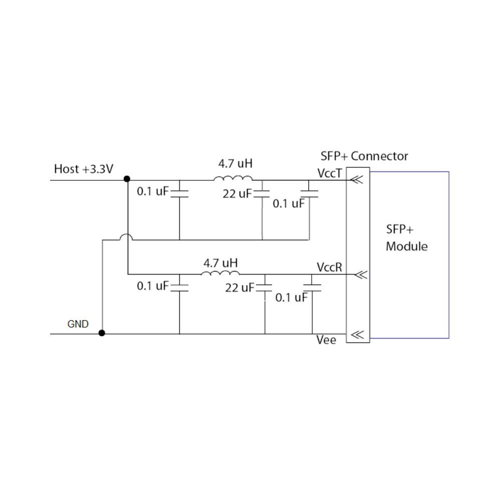
Host Board Power Supply Filters Circuit:

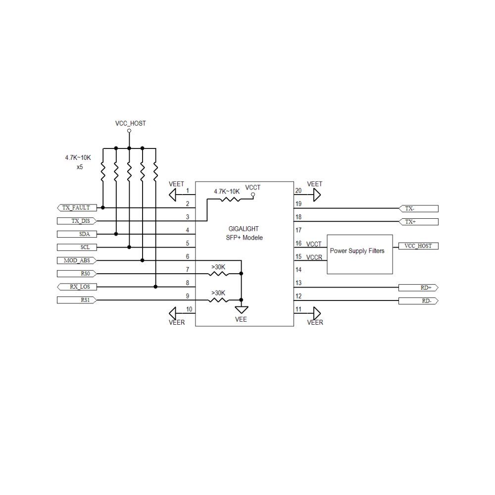
Host Module Interface:

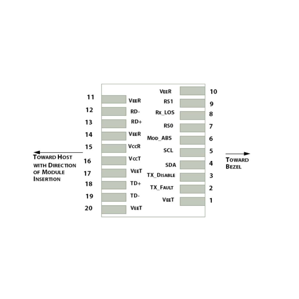
Pin Definitions:

| Pin |
Symbol |
Name/Description |
| 1 |
VEET [1] |
Transmitter Ground |
| 2 |
Tx_FAULT [2] |
Transmitter Fault |
| 3 |
Tx_DIS [3] |
Transmitter Disable. Laser output disabled on high or open |
| 4 |
SDA [2] |
2-wire Serial Interface Data Line |
| 5 |
SCL [2] |
2-wire Serial Interface Clock Line |
| 6 |
MOD_ABS [4] |
Module Absent. Grounded within the module |
| 7 |
RS0 [5] |
Rate Select 0 |
| 8 |
RX_LOS [2] |
Loss of Signal indication. Logic 0 indicates normal operation |
| 9 |
RS1 [5] |
Rate Select 1 |
| 10 |
VEER [1] |
Receiver Ground |
| 11 |
VEER [1] |
Receiver Ground |
| 12 |
RD- |
Receiver Inverted DATA out. AC Coupled |
| 13 |
RD+ |
Receiver DATA out. AC Coupled |
| 14 |
VEER [1] |
Receiver Ground |
| 15 |
VCCR |
Receiver Power Supply |
| 16 |
VCCT |
Transmitter Power Supply |
| 17 |
VEET [1] |
Transmitter Ground |
| 18 |
TD+ |
Transmitter DATA in. AC Coupled |
| 19 |
TD- |
Transmitter Inverted DATA in. AC Coupled |
| 20 |
VEET [1] |
Transmitter Ground |
Notes:
[1] Module circuit ground is isolated from module chassis ground within the module.
[2].should be pulled up with 4.7k – 10k ohms on host board to a voltage between 3.15Vand 3.6V.
[3]Tx_Disable is an input contact with a 4.7 kΩ to 10 kΩ pullup to VccT inside the module.
[4]Mod_ABS is connected to VeeT or VeeR in the SFP+ module. The host may pull this contact up to Vcc_Host with a resistor in the range 4.7 kΩ to10 kΩ.Mod_ABS is asserted “High” when the SFP+ module is physically absent from a host slot.
[5] RS0 and RS1 are module inputs and are pulled low to VeeT with > 30 kΩ resistors in the module.
Optical Characteristics:
| Parameter |
Unit |
Values |
| Operating Reach |
m |
10K |
| Transmit |
| Center wavelength (range) |
nm |
1260 -1355 |
| Side Mode Suppression Ratio (min) |
dB |
30 |
| Launched power |
| – maximum |
dBm |
+0.5 |
| – minimum |
dBm |
-8.2 Notes1 |
| – OMA |
dBm |
-5.2 |
| – OMA-TDP (min) |
dBm |
-6.2 |
| Transmitter and dispersion penalty |
dB |
0 Notes4 |
| Average launch power of OFF transmitter (max) |
dBm |
-30 |
| Extinction ratio (min) |
dB |
3.5 Notes2 |
| RIN12 OMA (max) |
dB/Hz |
-128 |
| Optical Return Loss Tolerance (min) |
dB |
12 |
| Receiver |
| Center wavelength (range) |
nm |
1260-1355 |
| Receive overload (max) in average power1 |
dBm |
0.5 |
| Receive sensitivity (min) in average power1 |
dBm |
-14.4 Notes3 |
| Receiver sensitivity (max) in OMA (footnote 2) |
dBm |
-12.6 Notes3 |
| Receiver Reflectance (max) |
dB |
-12 |
| Stressed receiver sensitivity (max) in OMA2 |
dBm |
-10.3 |
| Vertical eye closure penalty (min)3 |
dB |
2.2 |
| Stressed eye jitter (min)2 |
UIp-p |
0.7 |
| Receive electrical 3dB upper cutoff frequency (max) |
GHz |
12.3 |
| Receiver power (damage, Max) |
dBm |
1.5 |
| Notes:
1. The optical power is launched into SMF
2. Measured with a PRBS 231-1 test pattern@10.3125Gbps
3. Measured with a PRBS 231-1 test pattern@10.3125Gbps BER≤10-12
4. In G.652 and G.655(NDSF) |
Low Speed Characteristics:
| Parameter |
Symbol |
Min. |
Typical |
Max |
Unit |
| Power Consumption |
|
|
|
1 |
W |
| TX_Fault,RX_LOS |
VOL |
0 |
|
0.4 |
V |
| VOH |
Host_Vcc-0.5 |
|
Host_Vcc+0.3 |
V |
| TX_DIS |
VIL |
-0.3 |
|
0.8 |
V |
| VIH |
2.0 |
|
VCCT+0.3 |
V |
| RS0,RS1 |
VIL |
-0.3 |
|
0.8 |
V |
| VIH |
2.0 |
|
VCCT+0.3 |
V |
Electrical Characteristics:
| Parameter |
Symbol |
Min. |
Typical |
Max |
Unit |
Notes |
| Data Rate |
|
1.250 |
10.3125 |
– |
Gbps |
|
| Power Consumption |
|
– |
|
1000 |
mW |
|
| Transmitter |
| Single Ended Output Voltage Tolerance |
|
-0.3 |
– |
4.0 |
V |
|
| Common Mode Voltage Tolerance |
|
15 |
– |
– |
mV |
|
| Tx Input Diff Voltage |
VI |
400 |
|
1600 |
mV |
|
| Tx Fault |
VoL |
-0.3 |
|
0.4 |
V |
At 0.7mA |
| Data Dependent Input Jitter |
DDJ |
|
|
0.10 |
UI |
|
| Data Input Total Jitter |
TJ |
|
|
0.28 |
UI |
|
| Receiver |
| Single Ended Output Voltage Tolerance |
|
-0.3 |
– |
4.0 |
V |
|
| Rx Output Diff Voltage |
Vo |
300 |
|
850 |
mV |
|
| Rx Output Rise and Fall Time |
Tr/Tf |
30 |
|
|
ps |
20% to 80% |
| Total Jitter |
TJ |
|
|
0.70 |
UI |
|
| Deterministic Jitter |
DJ |
|
|
0.42 |
UI |
|
Recommended Operating Conditions:
| Parameter |
Symbol |
Min. |
Typical |
Max |
Unit |
| Power Supply Voltage |
VCC |
3.135 |
3.300 |
3.465 |
V |
| Operating Case Temperature (Standard) |
TC |
0 |
25 |
70 |
°C |
Absolute Maximum Ratings:
| Parameters |
Symbol |
Min. |
Max. |
Unit |
| Power Supply Voltage |
VCC |
0 |
+3.6 |
V |
| Storage Temperature |
Tc |
-40 |
+85 |
°C |
| Operating Case Temperature (Standard) |
Tc |
0 |
+70 |
°C |
| Relative Humidity |
RH |
5 |
95 |
% |
| RX Input Average Power |
Pmax |
– |
0 |
dBm |
Compliance Data:
| Feature |
Agency |
Standard |
Certificate / Comments
|
| Laser Safety |
FDA |
CDRH 21 CFR 1040 and Laser Notice No. 50 |
1120292-000 |
| Product Safety |
UL |
UL and CUL EN60950-2:2007 |
E347511 |
| Environmental protection |
SGS |
RoHS Directive 2002/95/EC |
GZ1001008918/CHEM |
| EMC |
WALTEK |
EN 55022:2006+A1:2007
EN 55024:1998+A1+A2:2003 |
WT10093759-D-E-E |


